Deposition basic information
Deposition describes a variety of methods that are used in micro- and nanofabrication to produce thin films and coatings. The TDSU 1 runs different systems for directed as well as conformal deposition of metal, dielectric and Si-based layers.
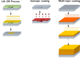
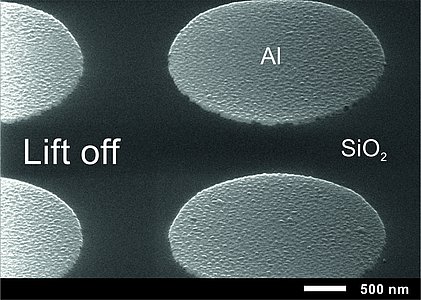
The evaporation and sputtering systems aim for directed deposition of metals and dielectrics. Depending on the tool they are designed to support micro structuring processes such as lift off, angle dependent or ion assisted deposition.
The plasma enhanced chemical vapour deposition (PECVD) is used to grow conformal Si-based active as well as isolation and passivation layers. It yields to relatively fast deposition rates while maintaining the film quality.
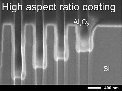
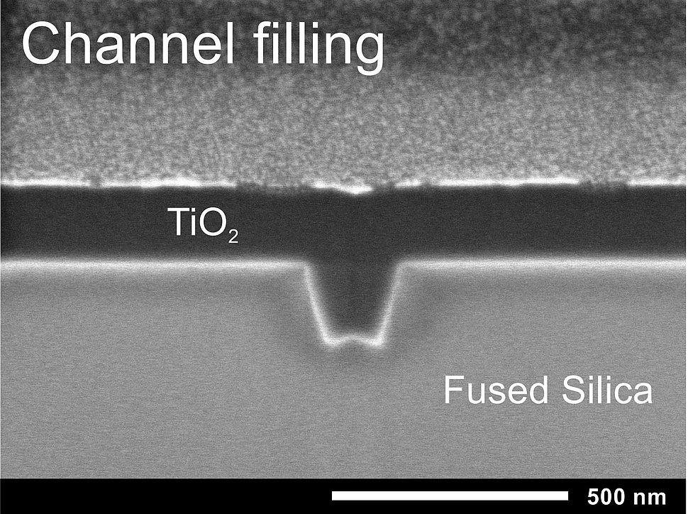
The atomic layer deposition (ALD) is the best choice for thin film high aspect ratio coatings. Sequential pulsing with precursors allows a self-limiting growth process which provides high quality thin film layers with precise control of the thickness at an atomic level.
Equipment
MEB550 S (Plassys)
Directed physical deposition of metals
Available materials: Au, Ti, Al, Ag, Pt, Cr
Typical film thickness: 10 - 150 nm
System Features
- E-Beam evaporator with 6 x 15 cm3 pockets and max. 6 kW operating power
- Ion source with Ar and Ar/O2 gas for sample cleaning
- 4“rotation substrate holder including tilting option with an accuracy of 0.01°
- Samples from a few mm size up to 4“ wafers

Leybold Univex 400
Univex 400 (Leybold)
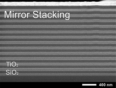
Directed physical deposition of dielectric materials (single layers or mirror stackings)
Available materials: MgF2, TiO2, SiO2
Typical film thickness: single layer10 - 300 nm and mirrors up to 2.5 µm
System Features
- E-Beam evaporator with 8 x 8cm3 pockets and max. 8 kW operating power
- 2 thermal evaporators with max. 8 V/ 400A
- Ion source with Ar and Ar/O2 gas for compressing, reactive evaporation and sample cleaning
- 6“ heated rotation substrate holder up to 350°C
- Samples from a few mm size up to 4“ wafers
Orion-5 (AJA Int.)
Directed physical deposition of metals and dielectrics with sputter-down geometry
Available materials: Ti, Cr, Au, Ag, ITO, TiO2, SiO2, Nb2O, SiN
Typical film thickness: 10 - 150 nm
System Features
- Ionautics HiPSTER6 6 KW HiPIMS source
- Trumpf TruPlasma DC 4002 for DC or pulsed DC plasma
- 300 W RF power source
- 50 W RF substrate bias
- Ar, N2 and O2 gas inlets for reactive and non-reactive sputtering
- Heated substrate table up to 600°C
- Samples from a few mm size up to 4" wafers
- Rohde & Schwarz RTB2004 oscilloscope for live monitoring
- Chamber fits five 2" targets simultaneously
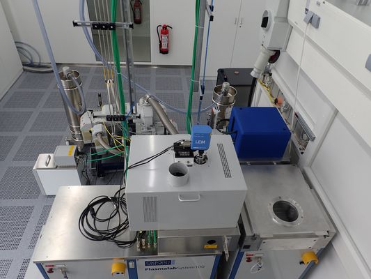
Plasmalab System 100 (Oxford Instruments)
Conformal chemical coating with silicon based materials
Available materials: Si3N4, SiO2, SiC
Typical film thickness: 50 - 1000 nm
System Features
- High frequency plasma up to 300 W and low frequency plasma up to 500 W
- Heated substrate table up to 400°C
- Samples from a few mm size up to 4“ wafers
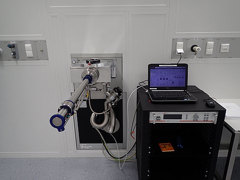
TFS 200 (Beneq)
Highly conformal chemical coating with oxide thin films
Available materials: Al2O3, TiO2, SiO2
Typical film thickness: 1 - 100 nm
System Features
- Thermal or Plasma-enhanced ALD
- Direct and remote capacitive coupled plasma up to 300 W
- Cold-wall vacuum chamber and hot-wall reaction chamber
- Substrate temperature: 25 - 500°C
- Samples from a few mm size up to 4“ wafers