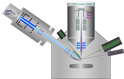
SEM and FIB basic information
The combination of SEM (Scanning Electron Microscopy) and FIB (Focus Ion Beam) systems, which are available at the TDSU1 facilities, allow the detailed imaging of processed micro- and nanostructures as well as the precise modification or patterning of materials in the nanometer range.
The Hitachi SEM system uses a focused beam of high-energy electrons to generate various signals at the surface of a solid sample. These signals, which are caused by electron-sample interactions, contain information about the topography and composition of the sample. The resolution of this equipment goes down to 1.2 nm.
The new surface imaging technique of the Zeiss Orion NanoFab FIB system allows an even better resolution scanning the surface with a focused helium ion beam instead. The extreme sharp ion source together with the large momentum of helium ions compared to electrons result in a sub nm probe size. Combined with a small beam divergence over a large penetration depth, this leads to a small interaction volume that enables a resolution of 0.5 nm.
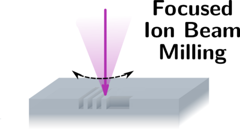
However the main focus of the FIB systems is nano-precise patterning of samples. The focused ion beam in this case is used to locally remove or in combination with a gas injection system deposit materials. The structure size and the fabrication speed highly depends on the used ions. Gallium and neon ions allow nano structuring at high speed and achieve a high throughput, while for the pattering of delicate sub 10 nm structures we use atomically sharp helium ion beam.