Lithographie basic information
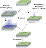
Lithography is typically used to expose the desired pattern. The resist material, which is sensitive to used radiation, is coated ontop of the sample and afterwards exposed to the radiation. After a development step the desired pattern exists as a resist structure which then can be processed further.
The TDSU 1 offers different possibilities for the lithography step based on electrons or photons for exposure. There are two direct writing systems available (Electron beam based Raith 150two and laser based DWL 66+) and a mask aligner MA6Gen4 for contact and proximity lithography.
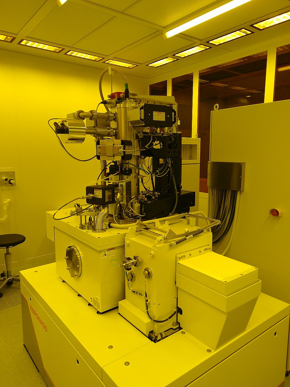
EBPG5200 (Raith GmbH)
-
Acceleration voltage 20, 50 and 100KV
-
100MHz fast data path channeling
-
Main field deflection to 20Bits resolution
-
100μm to 1mm write field size operation
-
Writing mode step and repeat with optimized stage setting
-
Minimum linewidth < 8nm
-
Stitch and overlay to < 10nm
Raith 150two (Raith GmbH)
-
Acceleration voltage EHT=0.1kV...30kV
-
Writing field WF=(500µm)² ... (2mm)²
-
Interferometrically controlled stage → Good write field stitching (accuracy 3σ < 40nm @WF 100μm, EHT 10kV, dwell time > 1μs)
-
Height sensing unit (accuracy σ < 1μm)
-
Overlay exposure (accuracy 3σ < 40nm @WF 100μm, EHT 10kV, dwell time > 1μs)
-
Writable area up to d=6", maximum sample size d=8"
-
Fixed Beam - Moving Stage writing mode for stitching free lines
-
Greytone exposure possible
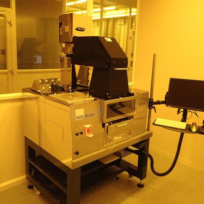
Mask Aligner: MA6Gen4 (Suess MicroTec)
-
Soft contact, hard contact, vacuum contact and proximty printing possible
-
MO optic for high uniformity, telecentric mask illumination, source decoupling, and the definition of the illuminating angular spectrum → high resolution or long working depth possible
-
Splitfield and single field topside alignment
-
Automatic wedge compensation
-
Hg lamp with 350W
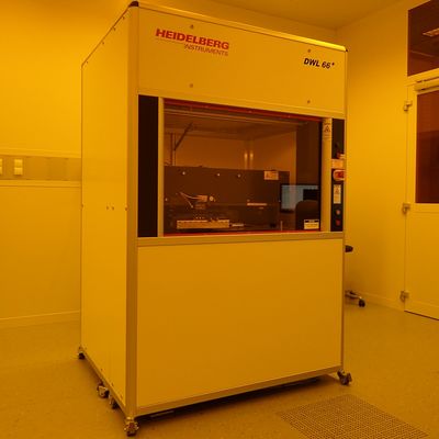
Laser lithography: DWL66+ (Heidelberg Instruments)
-
Semicoductor laser λ=405nm
-
Minimum feature size smaller 400nm
-
Greyscale exposure and compensation of the resist contrast curve
-
Overlay exposure with topside and backside alignment possible
-
Interferometrically controlled one axis air bearing stage stage
-
High writing speed due to acusto-optical deflector
-
Camera systems for overlay and metrology